by Fuding Ge
fudingge@yahoo.com
Copyright
( I am still working on it!!!)
Introduction
The noise in the circuitry can be roughly classified as inherent noise or interference noise.
Inherent noise can be reduced through careful design but never eliminated since this noise is due to the fundamental properties of the devices. Thermal, shot and flicker noise are examples of inherent noise. Inherent noise only slightly depends on the circuit routing or layout. However it can be significantly reduced by proper circuit design, such as changing the circuit structure or increase the power consumption.
Interference noise is due to the unwanted interaction between the circuit and the outside world, or between the different parts of the circuit itself. Examples are power supply noise on the ground wires (such as a 60-Hz hum) or electromagnetic interference (EMI), crosstalk, switching noise, ground bounce etc. This category of noise can be significantly reduced by proper routing, floorplan and layout.
From the source of noise viewpoint, they can be grouped as architecture/circuit
induced, substrate induced, device noise (thermal, flicker, shot), package
induced (lead inductance, package substrate, limited IO pads, current return
path) and power/ground induced, etc.
Inherent Noise in Solid State Devices
Thermal noise
Thermal noise (Johnson Noises) the
noise generated by thermal agitation of electrons in a conductor. It mainly
refers to resistor. As a result of the random thermal motion of the carriers,
a fluctuating voltage, Vnt appears across the resistor even
in the absence of a current from a external circuit. Using Norton equivalent,
thermal noise can described by an current, Int.
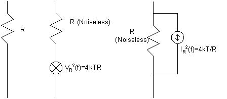
Vnt2=4KTRDf
Int2=4KTDf/R
Shot noise
Shot noise is the time-dependent fluctuations in electrical current
caused by the discreteness of the electron charge, is well known to occur
in solid-state devices, such as tunnel junctions, Schottky barrier diodes
and p-n junctions. Shot noise results from the fact that the current is
not a continuous flow but the sum of discrete pulses in time, each corresponding
to the transfer of an electron or hole through the conductor. Its spectral
density is proportional to the average current, I, and is characterized
by a white noise spectrum up to a certain cut-off frequency, which is related
to the time taken for an electron to travel through the conductor. In contrast
to thermal noise, shot noise cannot be eliminated by lowering the temperature.
In devices such as tunnel junctions the electrons are transmitted randomly
and independently of each other. Thus the transfer of electrons can be
described by Poisson statistics, which are used to analyze events that
are uncorrelated in time. For these devices the shot noise has its maximum
value at 2eI, where e is the electronic charge. However, shot noise is
absent in a macroscopic, metallic resistor because the ubiquitous inelastic
electron-phonon scattering smoothes out current fluctuations that result
from the discreteness of the electrons, leaving only thermal noise.
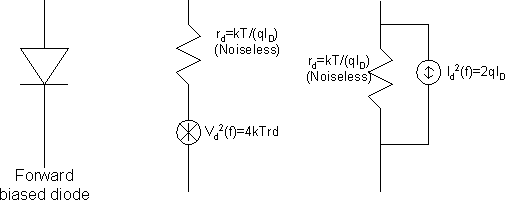
Shot noise can described by an current, Ins, which is superimposed on the nominal current, I. Ins is given by:
Ins2=2qIDf
Flicker noise
Flicker Noise (or 1/f noise) is the dominant noise source in MOSFET
devices at low frequencies. It is related to the extra energy states in
the Si-SiO2 interface. These states can trap and release electron
randomly, so fluctuation is produced. It is a relative slow process, most
of the fluctuation is at low frequency. It can be described by voltage
noise, Vnf, as:
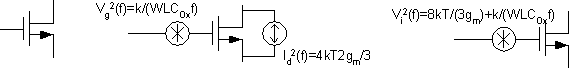
Vnf2=KDf/(CoxWL)
Noise models
for devices
The following is the modeling of resistor noise:
The following is the modeling of forward biased diode noise:
The following figure shows the modeling of BJT noise:

The following figure shows modeling of MOSFET noise:
Interference Noise: Coupling Noise in Mixed Signal Circuits
With the advance of technology, more and more devices are integrated in one chip. The so-called system-on-chip (SOC) consists of both high speed noisy digital blocks and high resolution quiet analog blocks. Then another category of noise, switching noise, through parasitic coupling, may become the limiting factor of the system.
The noise coupling between devices and blocks, mainly through interconnects, substrate, and power-supply lines. According to the coupling mechanism, it can be classified as capacitive or inductive coupling.
For capacitive coupling,
For inductive coupling,
In principle, any way that can reduce the paracitics (Cp, Lp) or the time derivative of the signals (dv/dt, dI/dt), will benefit the reduction of coupling noise. For example, the edge rate and drive strength of the IO buffers should be minimized to reduce the values of dv/dt and dI/dt respectively.
Parasitics can be reduced from different levels: system level, PCB level, package level and circuit level. From the point view of a circuit designer, parasitics reduction is much a layout related issue, for example, shielding signal, using guardring etc. As far as time derivative of signals is concerned, there are some special circuit architecture, or example, enhancement source-coupled logic (ESCL), can be used to reduce its value.
Noise coupled between interconnects
This noise is traditionally known as crosstalk. The effect is
due to the parasitic capacitance between any two parallel interconnects.
A voltage transient in one of the interconnects produce a noise peak in
the other interconnect. In mixed signal circuits, in order to reduce crosstalk,
care should be taken to separate the digital with the analog domains when
floorplanning the ICs, avoiding near long parallel analog and digital interconnects
lines. If totally separating the digital interconnect line with analog
one is impossible, for example in the sample-and hold part of a data converter,
use crossover instead of parallel. If necessary, coupled interconnect lines
should be shielded by the insertion of a third grounded line between them.
Substrate Noise
In principle, any switching node can reject noise to the substrate.
The noise in the substrate can also coupled into the devices. Understanding
the noise injection and reception mechanism can help their reduction.
Injection Mechanism: 1. Coupling across the PN junction formed between the devices and the substrate or well. 2. Noise in the power-supply line, which is used to bias the substrate, injected to the substrate through the contacts. This sort of noise injection can be reduced by paying attention to the parasitic capacitance, for example, reduce the line width if possible. 3. Other mechanisms, such as coupling between metal layer and substrate, hot carriers, impact ionization current.
Reception Mechanism: 1. Like the injection, the first one is the coupling across the PN junction and the substrate. 2. Through body effects. 3. Through the contacts: if supply lines powering the circuit also biasing the substrate, then noise is coupled between them through the contacts. Separated analog and digital substrate biasing lines. A high PSRR of the circuitry or fully differential architecture will help to reduce this noise coupling.
Generally speaking, the noise coupling between devices decreases with the increase of their distance. But this dependence on distance is related with the type of substrate (P-type or P-epi) [Aragones, 1999]. The presence of a backside bias contact to the substrate also reduces the noise.
Using guardring is another way to reduce substrate noise. The guardring
presents a low impedance return path to ground (or Vdd) in the disturbance
path, thus preventing noise from reaching the sensitive analog circuitry.
It is not necessary to have a ring fully surrounding the sensitive circuitry,
because the disturbance propagates along the straight line between the
coupled devices. A ring in the form of a barrier in the disturbance path
is enough, further increase the ring length does not help much. A small
opening in the ring (less than a few tens of microns) does not influence
its efficiency much. These openings can be important in the connectivity
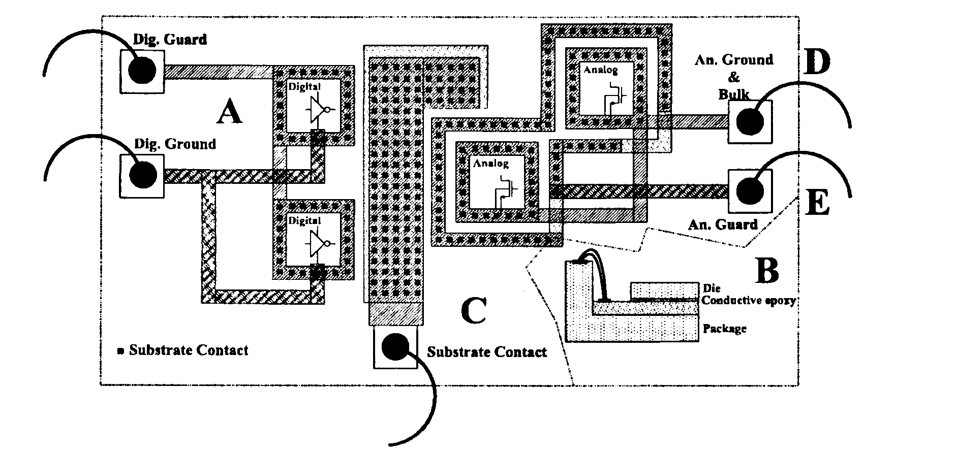
or routing problem. The following figure shows the biasing of an 3 level
guardring in a P-substrate N-well process. The middle ring is a P-type
tab while the outer ring are N-type.
Sometime triple well devices are available. Then using triple well in the sensitive cases could effectively reduce body effects and thus reduce noise coupling, but at the expense of larger area.
Using fully differential circuit design is an important to reduce power and substrate noise, at the expense of larger area and design complexity.
If possible, using current mode architecture to reduce noise.
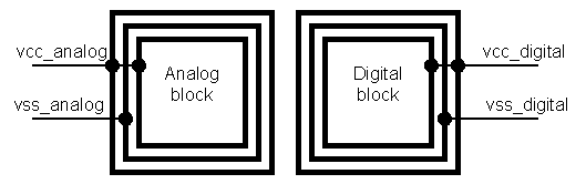
Proper substrate biasing also can reduce its noise coupling in a mixed signal circuit. When designing substrate biasing, a number of options can be used. The following figure shows four options. For (A), biasing the substrate of analog block using analog ground while biasing the digital substrate using digital ground. For (B), using analog ground to bias both analog and digital substrates. In this way, substrate acquires noise through contacts and this acquired noise has negative effects on the circuitry. For (C), using digital ground to bias both analog and digital substrate. Because analog ground is strongly contaminated with switching noise, and contacts will transfer this noise to substrate. For (D), a ground line dedicated exclusively for biasing substrate is used. It looks a perfect method, but it needs extra pins which mwans larger package, and extra contacts which may not be available.

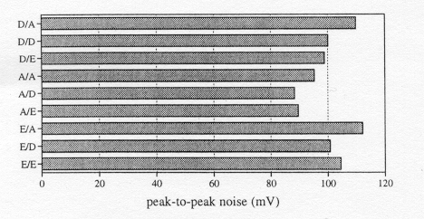
The following figures shows some simulation and measurement results
in [Aragones, 1999].
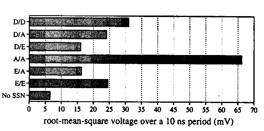
The above picture shows the simulation results of a mixed signal circuitry
on P-type substrate. The meaning of notation A/B is as following: the first
letter refers to circuit ground line (D for digital, A for analog) used
to bias the substrate in digital block and the second letter refers to
ground line used to bias analog substrate. For example, D/A means using
digital ground line to bias digital substrate and using analog ground line
to bias analog substrate. E/A means using a dedicated ground line to bias
digital substrate while using analog ground to bias analog substrate.
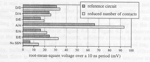
The above figure shows the effects of contact number of the ground lines.
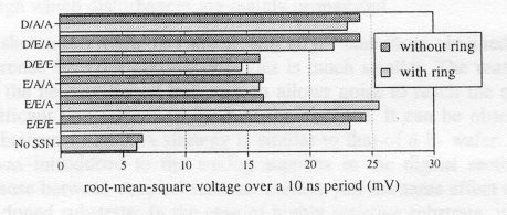
For the above figure, the third letter in the notation A/B/C refers
to the ground line used to bias the guardring.
The above is their measurement results.
Using same power supply lines to bias both analog and digital blocks should be avoided. Separated power supply line for digital and analog blocks is necessary for a low noise mixed signal circuit. Using digital power supply lines to bias digital parts and using analog lines to bias analog parts can reach required noise level, in some cases. If further noise reduction is required, a separated power line, exclusively for biasing analog circuitry, can be used, at the expense of area, routing, and more pins.
Separate analog and digital voltage regulator can be used. Filtered analog voltage regulator is another good idea.
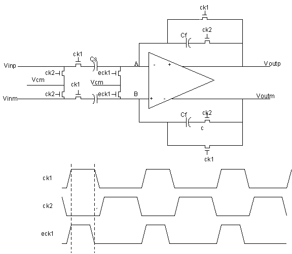
In a mixed signal circuitry, such as sample-and-hold circuits, when digital circuits is clocked, substrate noise is injected, and when when the noise is picked up when sampling, so clocking analog before digital is a good way to minimize noise coupling. The following figure shows an example:
From noise point view, the edge rate and drive strength of the IO buffers should be minimized, which we already mentioned above [Senthinathan, 1993].
There are some other proposals for substrate noise reduction, such as noise compensation [Sekiguchi, 1995]. The basic idea underlie this method is that: in some circuits, substrate noise is originated by certain particular items like large drivers, especially those of digital output pads, which usually toggle simultaneously. If we assume that the noise produced by a larger transistor is mainly injected to the substrate through the junction capacitance, it will be true that the noise peak produced by a 1 to 0 logic transition has a sign opposite to the noise peak produced by a 0 to1 transition. So adding dummy devices, counter phase switching in respect to the original noisy ones, then noise produced by both ones will cancel out. But there are some practical difficulties that makes this method unattractive and inefficient, such as there are no two complementary waweforms, so a 100% cancellation could never be achieved. The circuits has too small tolerance to switching skew, and it is difficulty to fix this skew.
Another proposal, active guard with an opamp with negative feedback,
is to sense noise waveform and produce a complementary waveform so both
cancel each out [Makie-Fukuda, 1995].
Switching Noise
Switching noise is also known as delta-I noise due to
mechanism that generating this type of noise, Vn =
LpdI/dt. The existence of parasitic inductance is
due to the package pins and bond wires and the whole power distribution
network. The on-chip power supply network inside an IC is mainly resistive.
The noise, generated by digital gates switching, is present in the power
supply line. The noise can transmit to other digital or analog blocks connected
to the same power supply line. The basic ideas underlie the reduction of
switching noise is to reduce parasitic inductance and isolation of the
noisy blocks from the quiet blocks such as using different power supply
line for the noisy circuitry (usually digital) and quiet one (usually analog).
Here we only discuss circuitry that reduce the value of dI/dt, based on
current consumption waveform shaping and power supply network design.
The first is the constant current consumption logic, which is originated from the emitter coupled logic (ECL) in BJT and current steering logic (CSL) in CMOS. The main disadvantage of this type of low noise solution is its static power consumption and non-standard logic level. This sort of logic includes Enhancement Source-Coupled Logic (ESCL) [Kiaei,1990][ Maleki, 1992], Folded Source-Coupled Logic (FSCL) [Allstot, 1993] [Sailesh, 1992]. Some researchers proposed current-balanced logic [Albuquerque, 1999] [Albuquerque, 2000]. According to the authors, with respect to CSL, CBL circuits can achieve the same degree of noise reduction and have improved performance (wider noise margins, lower delay) and reduced area for the same supply voltage and current, in addition to simpler circuit routing.
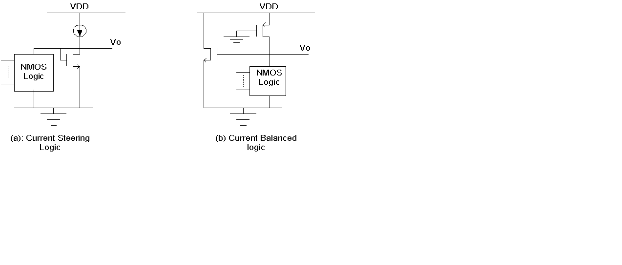
The following figure shows the function blocks of CSL and CBL.
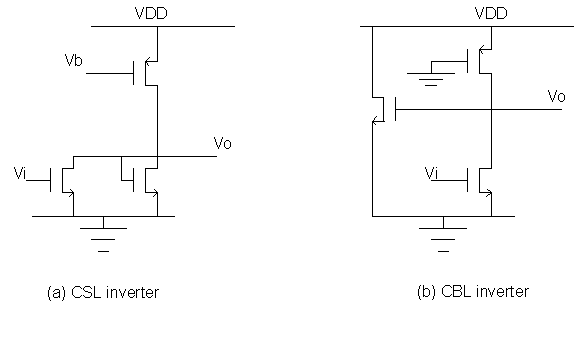
The following figures show a CSL and CBL inverter.
Switching noise can be reduced through proper decoupling capacitors. The inserting of decoupling capacitors is to compensate for the inductive nature of the conductors from different frequency. The same structure found at board level can be applied, scaled on Mulitchip Modules (MCM) level. But attentions must be paid to the possible oscillation produced by the LC circuit formed by the package inductance and the decoupling capacitors. This oscillation can be attenuated by resistance. The damping factor is given by:
x = R(C/L)1/2/2
Package Noise
Package inductance induced noise is a significant noise source for
mixed signal circuitry. The methods to reduce this noise includes isolated
analog/digital power and ground package substrate, sufficient pins for
analog and digital power pins as well as use low-inductance package bond-wires.
There are two alternatives for minimizing package inductance. First, several
package terminals dedicated to supply voltage can be used. In a first order
of approximation, the final value of the inductance will be the inductance
of single terminal divided by the number of supply terminals. If increasing
power supply pins is not sufficient or not cost-effective the type of package
must be replaced by another with a smaller terminal inductance. The next
table shows some package type and their typical inductance and capacitance
[Aragones, 1999].
| Package | Typical Inductance | Typical capacitance |
| DIP 68 plastic | 35 nH | 4.0 pF |
| DIP 68 Ceramic | 20 nH | 7.0 pF |
| SMT 68 | 7.0 nH | 2.0 pF |
| PGA 68 | 7.0 nH | 2.0 pF |
| PGA 256 | 15.0 nH | 5.0 pF |
| DIP 18 plastic | 13.7 nH | |
| SOIC 18 | 8.5 n | |
| QSOP 18 | 3.6 nH | |
| BGA | 3.0 nH | |
| Wire bond | 1.0 nH | 1.0 pF |
| Solder ball | 0.1 nH | 0.5 pF |
[Albuquerque, 2000] Edgar Albuquerque and Manuel Silva, "A comparative
study of low-noise logic cells for mixed mode integrated circuits", IEEE
International Symp. Circuits and System, 2000, May 28-31, Geneva, Switzerland,
V73-V76
[Allstot, 1993] D.J. Allstot, S.H. Chee, S. Kiaei, and Manu Shrivastawa, "Folded Source-Coupled Logic vs. CMOS Static Logic for Low-Noise Mixed-Signal ICs", IEEE Tr on Circuits and Systems-I, Vol 40, No.9, Sep 1993, pp553-563
[Aragones, 1999] Xavier Aragones, Jose Luise Gonzalez and Antonio Rubio, "Analysis and Solutions for Switching Noise Coupling in Mixed-Signal ICs," Kluwer Academic, Boston, 1999
[Gonzalez, 1995] J.L. Gonzales, and A. Rubio, "TCMOS: Low noise power supply technique for digital ICs", Electronics Letters, Vol.31, No 16, pp 1338-1339, 1995
[Johns, 1997] David Johns, Ken Martin, "Analog Integrated Circuit Design," John Wiley & Sons, New York, 1997
[Kiaei,1990] S. Kiaei, S.H. Chee, D.J. Allstot, "CMOS source coupled logic for mixed-Mode VLSI", Proc. IEEE Int. Symp. Circuits and system, 1990, pp1608-1611
[Makie-Fukuda, 1995] K Makie-Fukuda, S. Maeda, T. Tsukada, T. Matsuura, "Sunstrate noise reduction using active guard band filters in Mixed signal Integrated Circuits", Symposium on VLSI Circuits Digest of Technical papers, pp 33-34, 1995
[ Maleki, 1992] M. Maleki, and S. Kiaei, "Enhancement Source-Coupled Logiic for Mixed-Mode VLSI CIrcuits", IEEE Trans. on Circuits and Systems-II, Vol39, no.6, June 1992, pp399-401
[Sekiguchi, 1995] T. Sekiguchi, M. Horiguchi, T. Sakata, Y. Nakagoma, S. Ueda, M. Aoki, "Low-Noise, High-speed Data Transimission Using a Ringing-Canceling Output buffer", IEEE J. Solid-State Circuits, Vol 30, no.12, pp 1569-1574, December 1995.
[Senthinathan,
1993] R Senthinathan, J.L. Prince, "Application Specsific CMOS Output
Driver Circuit Design techniques to Reduce Simultaneous Switching noise",
IEEE J. Solid-State Circuits, Vol 28, no.12, pp 1383-1388, December 1993.
![]()
![]()
![]()
![]()
![]()
 visitor to this page. Thanks.